Нет товаров
Характеристики
| Тип корпуса | SOT-23 (6 лапок) |
| Шкаф | 01 |
| Бокс | 00 |
| Ячейка | 04 |
Описание
FEATURES Low On Resistance 2.5 Max <0.6 On Resistance Flatness Dual V or Single 5.5 V Supplies Rail-to-Rail Input Signal Range Tiny 6-Lead SOT-23 and 8-Lead Micro-SOIC Packages Low Power Consumption TTL/CMOS-Compatible Inputs APPLICATIONS Automatic Test Equipment Power Routing Communication Systems Data Acquisition Systems Sample and Hold Systems Avionics Relay Replacement Battery-Powered Systems GENERAL DESCRIPTION
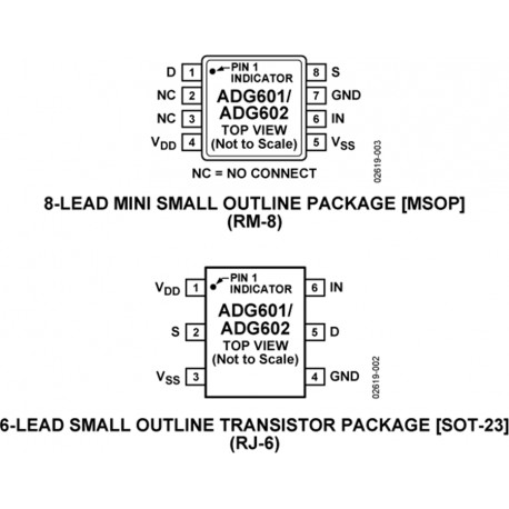
The ADG601/ADG602 are monolithic CMOS SPST (Single Pole, Single Throw) switches with On Resistance typically less than 2.5. The Low On Resistance flatness makes the ADG601/ ADG602 ideally suited to many applications, particularly those requiring low distortion. These switches are ideal for replacements for mechanical relays because they are more reliable, have lower power requirements, and package size is much smaller. The is a normally open (NO) switch, while the ADG602 is normally closed (NC). Each switch conducts equally well in both directions when ON, with the input signal range extending to the supply rails. They are available in tiny 6-lead SOT-23 and 8-lead MicroSOIC packages.
Low On Resistance (2 typical) Dual V or Single 5.5 V Supplies Tiny 6-lead SOT-23 and 8-lead Micro-SOIC Packages Rail-to-Rail Input Signal Range
Information furnished by Analog Devices is believed to be accurate and reliable. However, no responsibility is assumed by Analog Devices for its use, nor for any infringements of patents or other rights of third parties that may result from its use. No license is granted by implication or otherwise under any patent or patent rights of Analog Devices. One Technology Way, P.O. Box 9106, Norwood, MA 02062-9106, U.S.A. Tel: 781/329-4700 www.analog.com Fax: 781/326-8703 © Analog Devices, Inc., 2001
Parameter ANALOG SWITCH Analog Signal Range On Resistance (RON) On-Resistance Flatness (RFLAT(ON)) LEAKAGE CURRENTS Source OFF Leakage IS (OFF) Drain OFF Leakage ID (OFF) Channel ON Leakage ID, IS (ON) DIGITAL INPUTS Input High Voltage, VINH Input Low Voltage, VINL Input Current IINL or IINH CIN, Digital Input Capacitance DYNAMIC CHARACTERISTICS tON tOFF Charge Injection Off Isolation Bandwidth dB CS (OFF) CD (OFF) CD, CS (ON) POWER REQUIREMENTS IDD ISS
NOTES 1 Temperature range is as follows: B Version: to +85 °C. 2 Guaranteed by design, not subject to production test. Specifications subject to change without notice.
VDD +5.5 V, VSS V/+4.5 V; Test Circuit V/+4.5 V; Test Circuit 4.5 V; Test Circuit 3 V min V max
Parameter ANALOG SWITCH Analog Signal Range On Resistance (RON) On-Resistance Flatness (RFLAT(ON)) LEAKAGE CURRENTS Source OFF Leakage IS (OFF) Drain OFF Leakage ID (OFF) Channel ON Leakage ID, IS (ON) DIGITAL INPUTS Input High Voltage, VINH Input Low Voltage, VINL Input Current IINL or IINH CIN, Digital Input Capacitance DYNAMIC CHARACTERISTICS tON tOFF Charge Injection Off Isolation Bandwidth dB CS (OFF) CD (OFF) CD, CS (ON) POWER REQUIREMENTS IDD 0.001 1.0
NOTES 1 Temperature range is as follows: B Version: +85°C. 2 Guaranteed by design, not subject to production test. Specifications subject to change without notice.
VDD V/4.5 V; Test Circuit V/4.5 V; Test Circuit 1 V; Test Circuit 3


